Get In Touch
Every great partnership starts with a conversation.
Every great partnership starts with a conversation.

CONTACTS
Plot 16, Bayan Lepas Technoplex, Industrial Zone Phase 4, 11900 Bayan Lepas, Penang, Malaysia.

Maintaining consistent product quality is one of the biggest challenges in semiconductor manufacturing. As device complexity increases and component dimensions continue to shrink, manual inspection becomes less practical for high-volume production.
Automated Optical Inspection (AOI) uses advanced imaging technology and intelligent inspection algorithms to identify manufacturing defects quickly and consistently. Combined with vision inspection capabilities, AOI enables manufacturers to improve quality control, reduce inspection variability, and support more efficient production processes.
For semiconductor manufacturers in Malaysia, automated optical inspection has become an important part of modern back-end manufacturing, helping ensure products meet quality requirements before reaching the next production stage.
Visual defects that are difficult to detect manually can affect product quality, production yield, and downstream manufacturing processes.
An automated optical inspection system helps manufacturers inspect semiconductor devices with greater consistency by automatically analysing each product based on predefined inspection parameters.
Compared with manual inspection, AOI offers several advantages:
These benefits make AOI suitable for semiconductor manufacturers operating high-volume production environments.
Vision inspection refers to the use of cameras, optics, lighting, and image processing software to evaluate the condition of semiconductor devices during manufacturing.
Automated Optical Inspection is one application of vision inspection technology, where captured images are analysed to identify defects based on programmed inspection criteria.
This approach allows manufacturers to inspect products consistently while supporting automated production lines.
Modern vision inspection systems are capable of identifying various manufacturing defects before products proceed to the next production stage.
Typical inspection capabilities include:
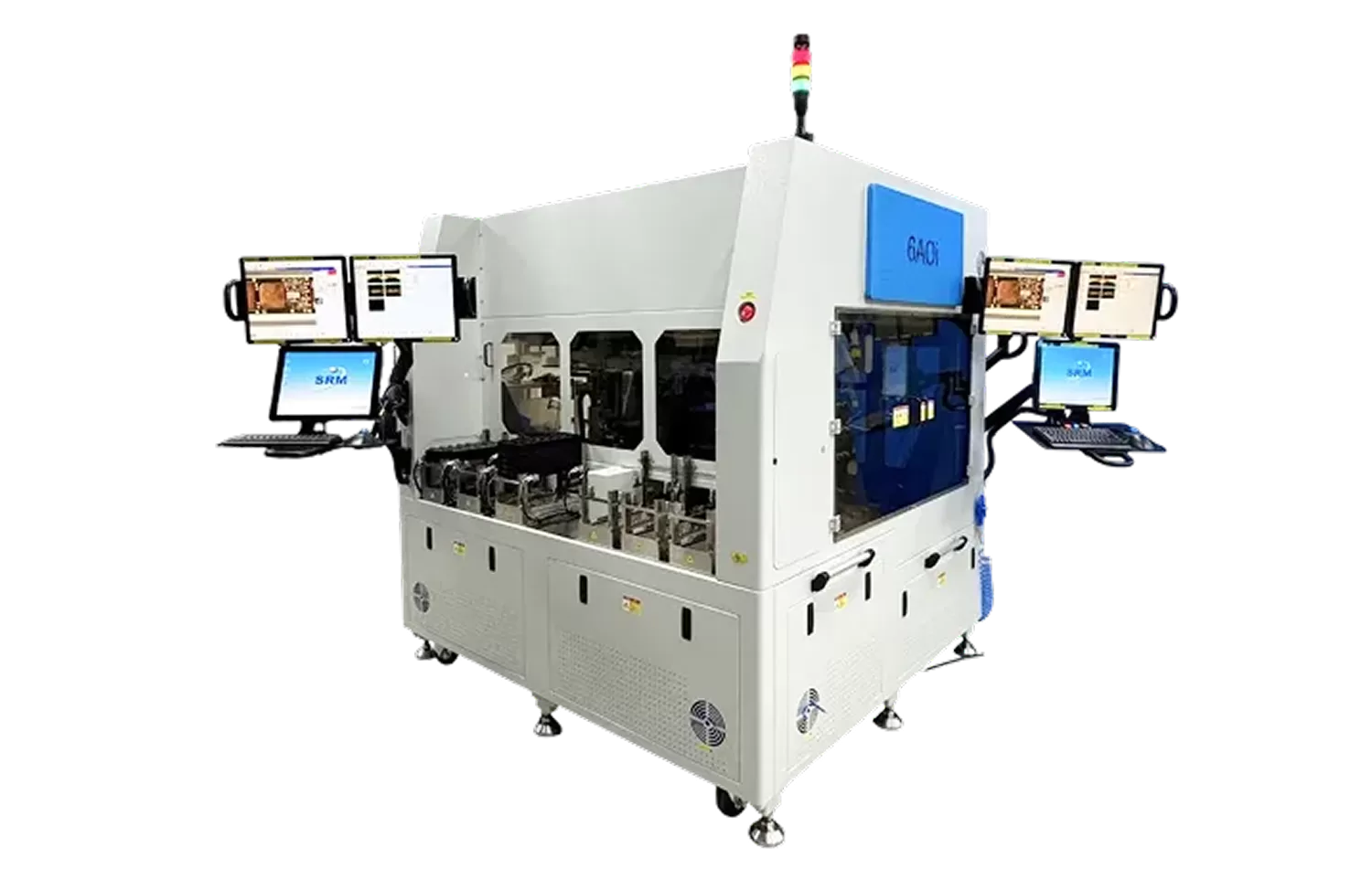
SRM’s 6-Sided AOI Inspection Handler is designed to inspect MOSFET and SiC modules using AI-powered vision inspection technology, supporting comprehensive inspection across multiple sides of the device.
Conventional inspection methods may only evaluate selected surfaces of a semiconductor package.
A six-sided inspection approach enables manufacturers to inspect multiple surfaces within a single automated process, improving overall inspection coverage and increasing the likelihood of identifying manufacturing defects before products continue through production.
For complex semiconductor packages, this provides additional confidence in product quality while reducing reliance on manual inspection.
Inspection is most effective when it complements automated device handling.
By integrating vision inspection with a semiconductor test handler, manufacturers can automate both device handling and inspection while maintaining stable production flow.
This integration helps reduce manual intervention, improve process consistency, and support higher production efficiency across back-end manufacturing operations.
Artificial intelligence is increasingly being incorporated into automated optical inspection systems to improve inspection accuracy and consistency.
AI-assisted image analysis can help identify subtle visual variations that may be difficult to detect consistently through manual inspection, while supporting faster decision-making during production.
Combined with automated handling, AI-powered inspection contributes to more reliable semiconductor manufacturing processes.
Selecting an automated optical inspection system requires more than evaluating inspection speed.
Manufacturers should consider:
Choosing an inspection solution that aligns with operational requirements helps manufacturers maintain efficient production while supporting long-term quality objectives.
As semiconductor manufacturing continues to advance, automated inspection has become an essential part of maintaining product quality and production efficiency.
By combining automated optical inspection with advanced technology for vision inspection Malaysia, manufacturers can identify defects more consistently, reduce manual inspection requirements, and support reliable high-volume production.
Integrated with automated semiconductor handling solutions, AOI plays an important role in strengthening quality control throughout the back-end manufacturing process.
Consistent inspection is essential for maintaining product quality in high-volume semiconductor manufacturing. SRM’s 6-Sided AOI Inspection Handler combines AI-powered vision inspection with automated handling to help manufacturers detect defects efficiently while supporting reliable back-end production processes.
Automated Optical Inspection (AOI) is an inspection process that uses cameras, lighting, and image processing technology to automatically detect visual defects on semiconductor devices during manufacturing, helping improve inspection consistency and production quality.
Vision inspection is the broader inspection technology that uses imaging systems to evaluate products, while Automated Optical Inspection (AOI) is a specific application of vision inspection that automatically detects manufacturing defects using predefined inspection criteria.
Depending on the inspection system, AOI can detect defects such as component misalignment, tilt, incomplete solder joints, missing components, connector pin coplanarity issues, surface warpage, and package cracks.
Six-sided inspection provides more comprehensive inspection coverage by evaluating multiple surfaces of a semiconductor package within a single automated process. This helps improve defect detection while supporting consistent quality control.
AOI enables fast and consistent inspection without relying on manual visual checks. When integrated with automated handling systems, it helps manufacturers maintain stable production flow, improve inspection repeatability, and support efficient back-end semiconductor manufacturing.