Get In Touch
Every great partnership starts with a conversation.
Every great partnership starts with a conversation.

CONTACTS
Plot 16, Bayan Lepas Technoplex, Industrial Zone Phase 4, 11900 Bayan Lepas, Penang, Malaysia.

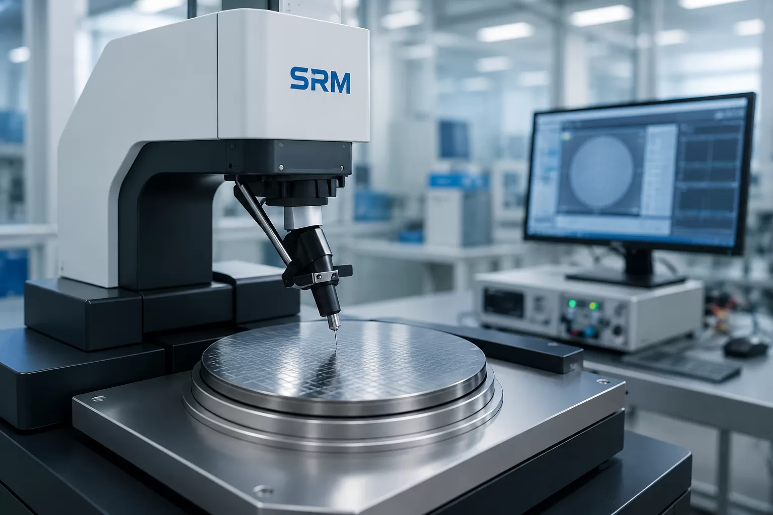
The semiconductor industry continues to evolve at a rapid pace, with quality control and process reliability standing as central pillars of competitive manufacturing. Among the technologies enabling this progress, the wafer prober has become an essential component for ensuring that every chip meets rigorous standards. As manufacturers face mounting pressure to achieve higher yields, tighter tolerances, and faster time-to-market, the role of wafer probers in quality assurance has never been more crucial. In this article, we examine the latest trends shaping wafer probing, the integration of automation and inspection, and how innovative solutions are transforming semiconductor quality control.
Wafer probers serve as the interface between delicate silicon wafers and advanced electrical test equipment. These highly engineered machines precisely position wafers and bring test needles or probes into accurate contact with each device site, enabling systematic electrical testing before chips are separated and packaged. The accuracy and reliability of wafer probing directly affect downstream yields and defect rates, making them foundational for quality management.
Modern wafer probers are engineered with robust motion control systems, temperature regulation capabilities, and adaptive probing force management. These elements ensure consistent contact, reduce the risk of wafer or die damage, and help uncover subtle electrical faults or process deviations early in the production flow. As semiconductor devices become smaller and more complex, the requirements for prober precision and versatility have intensified.
Recent years have seen a wave of automation and smart integration sweeping across the back-end semiconductor process. Wafer probers, once primarily manual or semi-automated, are now designed for full automation—enabling rapid, hands-free testing of large wafer batches. This shift is especially apparent in high-volume environments such as those operated by IDMs and OSAT companies.
Some of the most notable trends include:
As automation becomes deeply embedded in semiconductor manufacturing, wafer probers evolve from isolated test tools into integral nodes in a connected, intelligent production system.
Quality control extends beyond electrical testing—physical defects such as cracks, misalignment, warpage, and solder issues can also impact device reliability. Modern wafer probers increasingly incorporate advanced vision systems, including 2D, 3D, and multi-sided inspection, to detect subtle physical anomalies at the wafer level.
Artificial Intelligence (AI) is advancing these capabilities further. AI-powered inspection handlers, such as six-sided AOI solutions, are now able to identify a wide range of potential defects automatically. This enhances the accuracy of defect detection, reduces reliance on human inspectors, and improves traceability by integrating inspection data with electrical test results.
The synergy between probing and inspection means manufacturers can address both electrical and physical quality parameters in a single, unified workflow. This is particularly valuable for power semiconductor products, where device reliability is paramount.
Semiconductor packaging continues to diversify, driven by the needs of advanced applications such as automotive, communications, and consumer electronics. Wafer probers must accommodate a wide variety of wafer sizes, packaging types, and test configurations.
Key developments include:
This flexibility supports high-volume production plants as well as specialized engineering teams seeking unique automation and test solutions.
The ultimate objective of integrating advanced wafer probing is to enhance productivity while maintaining or improving quality standards. Features such as automated alignment, precise motion control, and seamless workflow automation reduce human error, accelerate throughput, and enhance traceability across the production lifecycle.
Leading equipment providers have introduced modular platforms that offer scalability and easy upgrade paths. These innovations help semiconductor manufacturers respond rapidly to changing device designs, production volumes, and quality expectations. By minimizing downtime and optimizing asset utilization, automated wafer prober systems contribute to a more agile and cost-effective manufacturing environment.
Furthermore, as reliability expectations rise in sectors such as automotive and power electronics, the role of wafer probers in detecting early-stage failures and latent defects becomes even more critical.
Wafer probers are at the heart of the semiconductor industry’s push for improved quality control, higher yields, and greater manufacturing efficiency. As automation, vision inspection, and AI technologies advance, the capabilities of wafer probing systems continue to expand. Manufacturers who leverage these trends stand to benefit from more reliable products, faster cycle times, and a stronger competitive position.
With the ongoing evolution of semiconductor devices and increasing demand for customized, high-performance solutions, the importance of choosing the right wafer prober partner is paramount. By combining innovative engineering, flexible automation options, and advanced inspection technologies, companies like SRM Integration (Malaysia) Sdn Bhd are helping to shape the future of quality control in semiconductor manufacturing.
A wafer prober is a precision machine that positions silicon wafers and brings test probes into contact with individual device sites, enabling electrical testing before chip packaging. It is vital for early defect detection, ensuring only functional devices progress through the manufacturing process, thereby improving yield and reliability.
Automation has enabled wafer probers to operate with minimal manual intervention, increasing throughput and consistency. AI-powered vision inspection systems integrated with probers can now detect a wider range of defects more accurately, reducing reliance on human inspection and improving overall quality assurance.
Turret handlers are high-speed rotary systems that automate the loading and unloading of devices during testing. When used alongside wafer probers, they support continuous, high-throughput operations, providing efficient handling of various IC packages and enabling seamless integration with testing and inspection processes.
Supporting multiple input formats allows wafer probers to handle different device types and packaging methods efficiently. This flexibility is crucial for manufacturers facing diverse customer requirements and enables smooth transitions between process steps like sorting, testing, and packaging.
Advanced wafer probers with integrated automation and inspection capabilities help detect defects early, minimize manual errors, and enable faster cycle times. This leads to higher yields, less rework, and more efficient use of resources, ultimately reducing overall production costs for semiconductor manufacturers.
Unlock new levels of precision, efficiency, and reliability in your semiconductor manufacturing with SRM Integration (Malaysia) Sdn Bhd. Our advanced wafer prober solutions, high-speed handlers, and AI-powered inspection systems are engineered to meet the demands of modern production environments. Partner with us to achieve superior quality control, higher yields, and seamless automation tailored to your requirements.